


The nRF54L15 is a next-generation low-power wireless SoC from Nordic Semiconductor, designed for advanced Bluetooth LE and IoT applications. This article walks you through the basic steps required to compile and program the nRF54L15 using the Nordic SDK, VS Code, and a J-Link debugger.
Before programming the nRF54L15, you need to connect the development board to a J-Link debugger. This connection is required for flashing and debugging.
.jpg)
.jpg)
Development Board | J-Link |
VCC | VCC |
GND | GND |
SWCLK | SWCLK |
SWDIO | SWDIO |
After wiring, ensure that all connections are stable and correct. Once connected, the board is ready for programming.
.jpg)
After completing the hardware connection, proceed with the software setup.
Launch VS Code, make sure the Nordic SDK is properly installed and configured.
Then compile and flash the firmware according to the SDK configuration.
(Detailed steps can be followed in the tutorial video.)
To quickly verify functionality, you can create a Nordic official slave example within the SDK and test data transmission via UART.
.jpg)
In the SDK example list, choose a slave (peripheral) example provided by Nordic.
.jpg)
Add the required build and compilation tools as prompted by the SDK environment.
.jpg)
Choose the corresponding nRF54L15 Development Kit (DK) as the target hardware platform.
.jpg)
Use the default compilation options and start the build process.
Wait until the compilation completes successfully.
.jpg)
You can manually define the UART pins in the project configuration.
Tip: It is recommended to use P1.xx pins for UART to ensure better flexibility and compatibility.
.jpg)
.jpg)
Once programming is successful, the example application will run as expected.
UART TX pin: P1.04
UART RX pin: P1.05
In this setup:
A mobile phone acts as the master device
The nRF54L15 runs as a slave device
Data sent from the phone is received by the nRF54L15 and displayed through the UART serial output
This confirms that the firmware has been successfully compiled, flashed, and is functioning correctly.
Conclusion
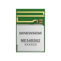
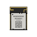
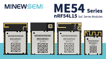
This guide demonstrates the complete programming and compilation workflow using the MinewSemi nRF54L15-ME54BS01 module and its corresponding development board as a practical example. From J-Link hardware connections to SDK configuration, example compilation, and UART data verification, the process provides a reliable reference for engineers getting started with the nRF54L15 platform.
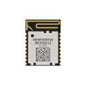
Beyond the ME54BS01, MinewSemi offers a full portfolio of nRF54L15-based wireless connectivity modules, designed to support different antenna options, form factors, and integration requirements. These modules are well-suited for a wide range of Bluetooth LE and next-generation IoT applications, enabling faster development cycles and easier migration from prototype to production.
Whether you are evaluating the nRF54L15 for a new design or scaling an existing product, MinewSemi’s nRF54L15 module lineup provides flexible, production-ready solutions to accelerate your development.